A defect in a semiconductor chip may be smaller than a human hair but can create big problems in your everyday life, from crippling your car’s steering to making your laptop more susceptible to hackers.
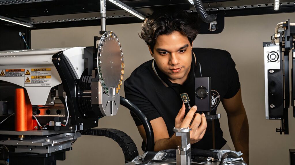
Nikhilesh Chawla, a Purdue University engineer, is working with university colleagues and scientists at the U.S. Department of Energy’s (DOE) Argonne National Laboratory on high-resolution imaging to better spot defects and speed up the existing inspection process during chip manufacturing.
“Looking at defects in semiconductors and being able to detect them quickly so that we can help the industry is a very important topic,” said Chawla, Purdue’s Ransburg Professor in Materials Engineering. “We’re hoping to accelerate the entire process by using new imaging techniques and faster algorithms.”
The research looks at several aspects of defects, including how they form and if any particular phase of semiconductor packaging is more susceptible to defects during the manufacturing process. Packaging refers to multiple chips that are connected electrically. Advanced packaging aims to revolutionize packaging by enabling complex functionality while reducing cost.
Chawla said the work is broken down into three areas, starting with high-resolution imaging that must be able to see the smallest defects possible. For that, he is working with X-ray imaging and X-ray tomography at the Advanced Photon Source, a DOE Office of Science user facility at Argonne, to create a 3D microstructure of the chip. Once defects are located, the technique works backward through the process to determine where the defects may have initially formed.
The second step utilizes artificial intelligence to make sure the detection technique is quicker and smarter with more efficient algorithms to process the imaging data and ensure automatic defect detection so the manufacturing process isn’t hindered.

“The third part is to understand which category of defects is going to cause trouble for the chip in the field,” Chawla said. “By understanding which ones are really going to cause problems in the device, we can catch them in the manufacturing cycle and prevent failures from happening with the customer.”
The team on this project also includes Purdue’s Charles Bouman, the Showalter Professor of Electrical and Computer Engineering and Biomedical Engineering; Greg Buzzard, professor of mathematics; and Hany Abdel-Khalik, professor of nuclear engineering, as well as Francesco de Carlo from Argonne, Erdogan Madenci from the University of Arizona, and Martin Gall from GlobalFoundries.
Purdue’s national leadership in microelectronics and semiconductors is a cornerstone of Purdue Computes—a comprehensive initiative that spans computing departments, physical AI, quantum science and semiconductor innovation. The university’s cutting-edge research, transformational investments in infrastructure and workforce development programs are setting a national benchmark for excellence and spearheading a growing semiconductor cluster in West Lafayette.
Chawla’s research with Argonne is being done as part of the National Science Foundation’s Future of Semiconductors program. Chawla said he expects the work to be published as early as the end of the year.
For industry, the technique could offer a new way of handling chip issues for semiconductors.
“The semiconductor industry is used to taking a defective component and cutting it up, which is very laborious and time-consuming, plus then you’ve also lost the part,” Chawla said. “With a nondestructive imaging technique, we’re hoping to have something to get snapshots of the chip structure as it’s going through the manufacturing process so you know the condition of a component.”
Data from this research could lead to future probability uses, such as using the imaging data to help determine the timeframe in which a defect could cause a device like a cell phone to fail.
Citation:
Cutting-edge imaging and faster algorithms for finding minuscule defects in semiconductor chips (2025, October 13)
retrieved 14 October 2025
from https://techxplore.com/news/2025-10-edge-imaging-faster-algorithms-minuscule.html
This document is subject to copyright. Apart from any fair dealing for the purpose of private study or research, no
part may be reproduced without the written permission. The content is provided for information purposes only.

